- 您现在的位置:买卖IC网 > Sheet目录2005 > LTC2240CUP-12#PBF (Linear Technology)IC ADC 12BIT 170MSPS 64-QFN
LTC2240-12
18
224012fd
APPLICATIONS INFORMATION
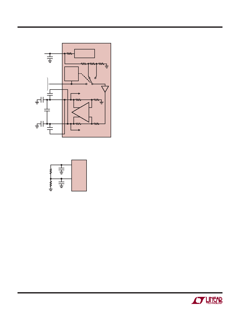
and REFLB for the low reference. The multiple output pins
are needed to reduce package inductance. Bypass capaci-
tors must be connected as shown in Figure 9.
Other voltage ranges in between the pin selectable ranges
can be programmed with two external resistors as shown
in Figure 10. An external reference can be used by ap-
plying its output directly or through a resistor divider to
SENSE. It is not recommended to drive the SENSE pin
with a logic device. The SENSE pin should be tied to the
appropriate level as close to the converter as possible. If
the SENSE pin is driven externally, it should be bypassed
to ground as close to the device as possible with a 1μF
ceramic capacitor.
Input Range
The input range can be set based on the application.
The 2V input range will provide the best signal-to-noise
performance while maintaining excellent SFDR. The 1V
input range will have better SFDR performance, but the
SNR will degrade by 5dB. See the Typical Performance
Characteristics section.
Driving the Encode Inputs
The noise performance of the LTC2240-12 can depend
on the encode signal quality as much as on the analog
input. The ENC+/ENC– inputs are intended to be driven
differentially, primarily for noise immunity from common
mode noise sources. Each input is biased through a 4.8k
resistor to a 1.5V bias. The bias resistors set the DC op-
erating point for transformer coupled drive circuits and
can set the logic threshold for single-ended drive circuits.
Any noise present on the encode signal will result in ad-
ditional aperture jitter that will be RMS summed with the
inherent ADC aperture jitter.
In applications where jitter is critical (high input frequen-
cies) take the following into consideration:
1. Differential drive should be used.
2. Use as large an amplitude as possible; if transformer
coupled use a higher turns ratio to increase the amplitude.
3. If the ADC is clocked with a sinusoidal signal, lter the
encode signal to reduce wideband noise.
4. Balance the capacitance and series resistance at both
encode inputs so that any coupled noise will appear at
both inputs as common mode noise. The encode inputs
have a common mode range of 1.2V to 2.0V. Each input
may be driven from ground to VDD for single-ended drive.
Figure 9. Equivalent Reference Circuit
Figure 10. 1.5V Range ADC
VCM
REFHA
REFLB
SENSE
TIE TO VDD FOR 2V RANGE;
TIE TO VCM FOR 1V RANGE;
RANGE = 2 VSENSE FOR
0.5V < VSENSE < 1V
1.25V
REFLA
REFHB
2.2μF
INTERNAL ADC
HIGH REFERENCE
BUFFER
0.1μF
224012 F09
LTC2240-12
2Ω
DIFF AMP
1μF
0.1μF
INTERNAL ADC
LOW REFERENCE
1.25V BANDGAP
REFERENCE
1V
0.5V
RANGE
DETECT
AND
CONTROL
VCM
SENSE
1.25V
2.2μF
8k
12k
0.75V
1μF
224012 F10
LTC2240-12
发布紧急采购,3分钟左右您将得到回复。
相关PDF资料
LTC2240IUP-10#PBF
IC ADC 10BIT 170MSPS 64-QFN
LTC2241IUP-10#PBF
IC ADC 10BIT 210MSPS 64-QFN
LTC2242IUP-10#PBF
IC ADC 10BIT 250MSPS 64-QFN
LTC2245IUH#TRPBF
IC ADC 14BIT 10MSPS 3V 32-QFN
LTC2249IUH#TRPBF
IC ADC 14BIT 80MSPS LP 32-QFN
LTC2251IUH#PBF
IC ADC 10-BIT 125MSPS 3V 32-QFN
LTC2253IUH#TRPBF
IC ADC 12BIT 125MSPS 3V 32-QFN
LTC2255CUH#TRPBF
IC ADC 14BIT 125MSPS 3V 32-QFN
相关代理商/技术参数
LTC2240CUP-12#TRPBF
功能描述:IC ADC 12BIT 170MSPS 64-QFN RoHS:是 类别:集成电路 (IC) >> 数据采集 - 模数转换器 系列:- 标准包装:1 系列:- 位数:14 采样率(每秒):83k 数据接口:串行,并联 转换器数目:1 功率耗散(最大):95mW 电压电源:双 ± 工作温度:0°C ~ 70°C 安装类型:通孔 封装/外壳:28-DIP(0.600",15.24mm) 供应商设备封装:28-PDIP 包装:管件 输入数目和类型:1 个单端,双极
LTC2240CUP-12-PBF
制造商:LINER 制造商全称:Linear Technology 功能描述:12-Bit, 170Msps ADC
LTC2240CUP-12-TR
制造商:LINER 制造商全称:Linear Technology 功能描述:12-Bit, 170Msps ADC
LTC2240CUP-12-TRPBF
制造商:LINER 制造商全称:Linear Technology 功能描述:12-Bit, 170Msps ADC
LTC2240IUP-10
制造商:LINER 制造商全称:Linear Technology 功能描述:10-Bit, 170Msps ADC
LTC2240IUP-10#PBF
功能描述:IC ADC 10BIT 170MSPS 64-QFN RoHS:是 类别:集成电路 (IC) >> 数据采集 - 模数转换器 系列:- 标准包装:1 系列:- 位数:14 采样率(每秒):83k 数据接口:串行,并联 转换器数目:1 功率耗散(最大):95mW 电压电源:双 ± 工作温度:0°C ~ 70°C 安装类型:通孔 封装/外壳:28-DIP(0.600",15.24mm) 供应商设备封装:28-PDIP 包装:管件 输入数目和类型:1 个单端,双极
LTC2240IUP-10#TRPBF
功能描述:IC ADC 10BIT 170MSPS 64-QFN RoHS:是 类别:集成电路 (IC) >> 数据采集 - 模数转换器 系列:- 标准包装:1 系列:- 位数:14 采样率(每秒):83k 数据接口:串行,并联 转换器数目:1 功率耗散(最大):95mW 电压电源:双 ± 工作温度:0°C ~ 70°C 安装类型:通孔 封装/外壳:28-DIP(0.600",15.24mm) 供应商设备封装:28-PDIP 包装:管件 输入数目和类型:1 个单端,双极
LTC2240IUP-10-PBF
制造商:LINER 制造商全称:Linear Technology 功能描述:10-Bit, 170Msps ADC